Low Latency True Random Number Generator.
Status: In Fabrication Stage
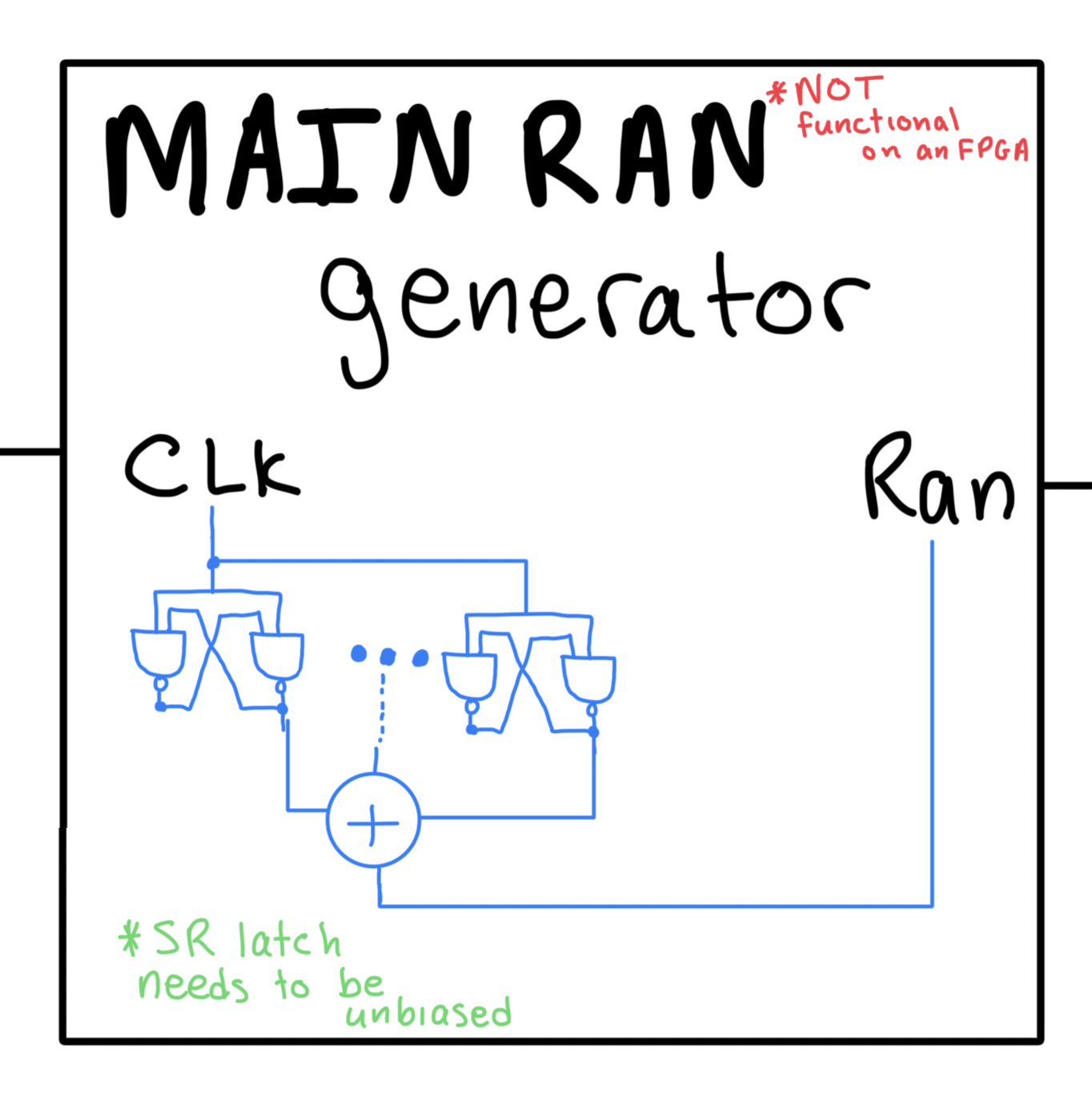
When I was taking 281 Digital Logic my first semester, I remember being tought about latches. Seeing the diagram of a latch, and seeing the truth table, I wasn’t able to trace the initial value. This got me curious. I knew that when you power the circuit up, it has to take on some value. It seemed to me that this value might be random. Looking into papers online about random numbers generators with latches, I got even more interested. The latch topology that really got my attention was very simple: an SR latch in which Set and Reset are connected to a clock. An SR latch’s Set and Reset are active low. But you can’t Set and Reset at the same time? When you drive Set and Reset both low, the NAND gates are forced to output 1 (~(x & 0) = 1). This is considered an invalid state for the latch as you can’t “Set” and “Reset” at the same time and both outputs of the latch can’t be the same as they should be inverted from each other. But what happens when both inputs simultaneously are put high? This becomes a sort of electric race condition. We use the clock to generate a bit on every positive edge. This requires special balancing and symmetry and can’t be auto routed by toolflow. This also means that it may not work on an FPGA (which it didn’t, but maybe manually routing the LUTs in the fabric might have different results. Acutally this was shown successful in this paper ).
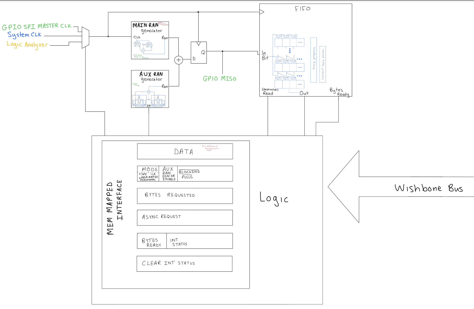
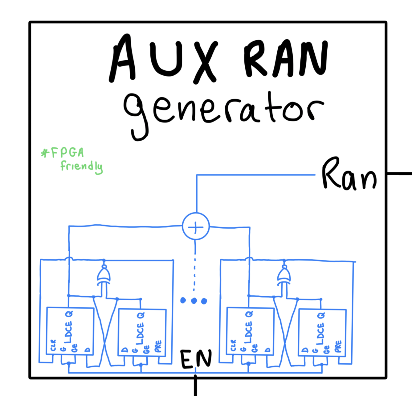
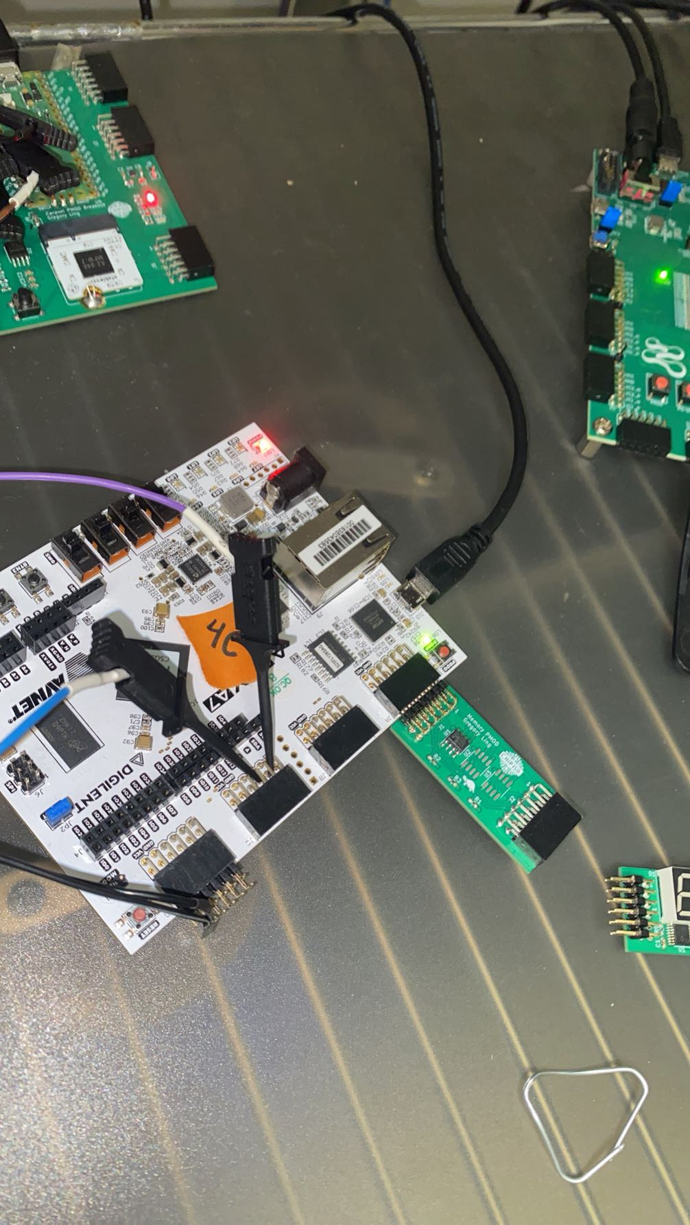
Having interest in digital design, and also being part of the ISU ChipForge club, I found this as a good opportunity to design a True Random Number Generator and have it fabricated. Extending it past just a raw bit generator, I made it into an embedded memory mapped peripheral including a FIFO, interrupt support, and an SPI mode. Two entropy sources are available, the primary entropy source using an array of the latches mentioned above, and an array of FPGA friendly dual latch random number generator topology, the auxiliary entropy source.
The whole design was prototyped on an FPGA (except for the primary entropy source not being random on the FPGA). I wrote firmware for the VexRiscv core to check functionality of my peripheral and to make a serial interface to where I can control and check results of my peripheral. I also wrote a testbench and used ModelSim for verification of the FIFO.
Primary Random Number Generator
Relevant Paper: Torii, N., Kokubo, H., Yamamoto, D. et al. ASIC implementation of random number generators using SR latches and its evaluation. EURASIP J. on Info. Security 2016, 10 (2016). https://doi.org/10.1186/s13635-016-0036-1
This topology of latch based random number generator can be found
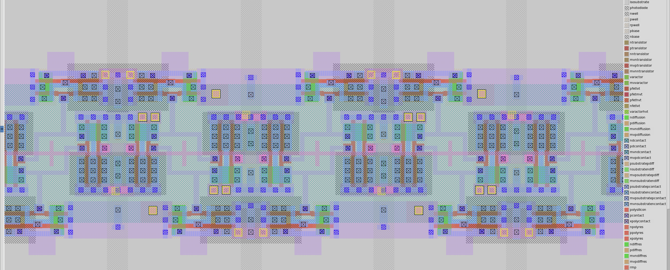
This was my first time doing analog layout in a chip. The PDK (sky130) had logic standard cells so it was a matter of finding a layout such that the traces and parasitics can all be symmetrical and balanced. I found that inverting and/or flipping the NAND gates allowed me to join two NAND gates in such a way where not only the traces inbetween them are equal, but also the same ports connect to the same other ports (for example, A connects to Y and Y connects to A on the other NAND, instead of A connecting to Y and Y connecting to B on the other NAND). A buffer was used very close so to not extend the trace further and have any nonsymmetries accumulate. A dummy buffer was added to the non utilized output of the latch so that the capacitances and parsitics can match on both traces within the latch.
This sort of layout introduced new challenges though: the checkered wells and power points. In a single latch, you have one NAND gate whose VDD is on top and whose GND is on bottom, another NAND gate whose GND is on top and whose VDD is on bottom. To make it even more interesting, a NAND gate’s VDD is adjacent to a buffer’s GND and a NAND gate’s GND is adjacent to a buffer’s VDD. To make this problem easier to deal with (or less harder), I decided to connect two latch units together by having it so a NAND sits side by side a NAND gate from the other latch where the VDD and GND of the two NAND gates are on the same level. A tap cell is put inbetween them so they can share wells. A buffer’s VDD side of one of the latches stiches to a buffer’s VDD side of another latch via a half tap cell (a nwell tap). A buffer’s GND side of one of the latches stiches to a buffer’s GND side of another latch via also a half tap cell (a pwell tap), but these buffers are more horizontally farther apart, so the half tap cell sits equidistance from the buffers and is bridged with metal1.
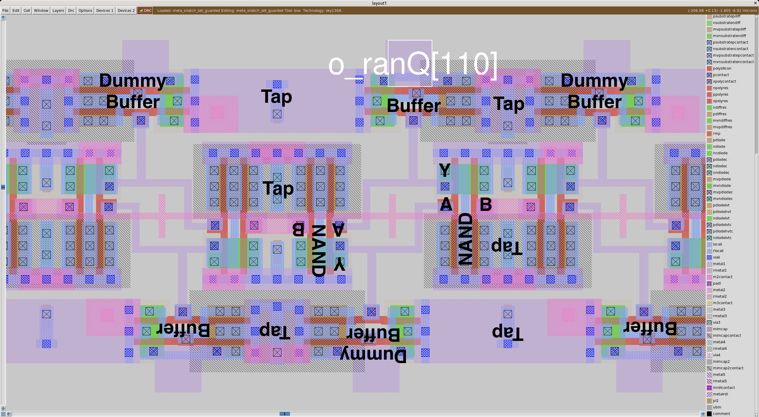
A ground rail is ran horizontally through the middle and power rails are ran vertically throughout.
Looking at this now, as I write this up, that clock going to 128 latches (so 256 logic gates) might have a huge capacitive load to drive. Buffers could maybe be added for future revisions. I’m hoping that the synthesis tools made the drive of the clock going to this analog block very strong.
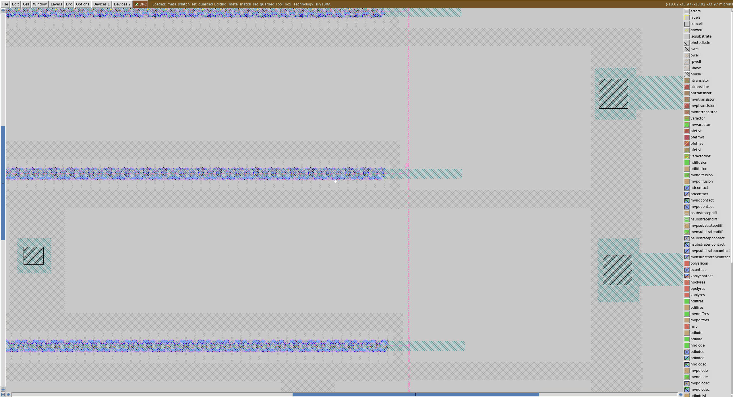
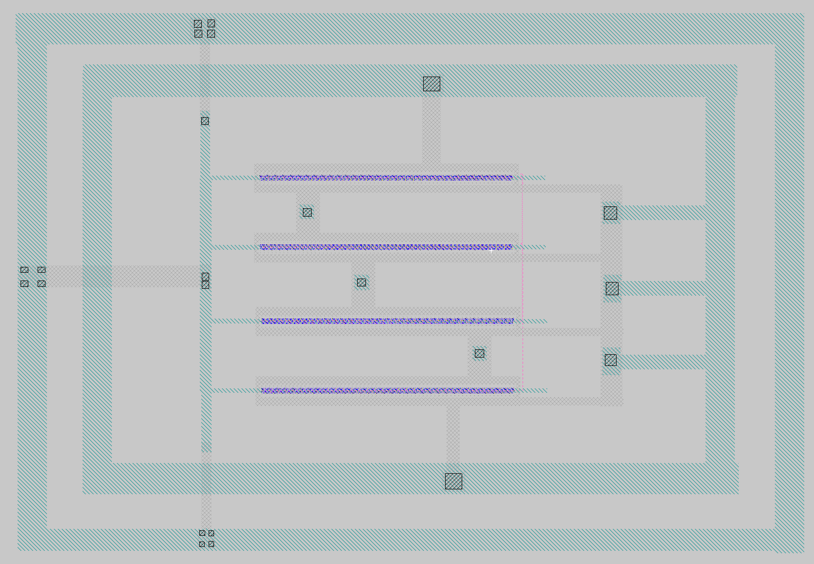
When I tried integrating this with my digital design, the place and route wasn’t able to succesfully place the power or ground so I made a guard ring to make it easier on the placement tool to find a place to drop power and ground.
Auxiliary Random Number Generator
Relevant Paper: M. M. Esen, Ş. Uzun and E. Göncü, “FPGA Latch Primitive based Efficient True Random Number Generators,” 2023 30th IEEE International Conference on Electronics, Circuits and Systems (ICECS), Istanbul, Turkiye, 2023, pp. 1-8, doi: 10.1109/ICECS58634.2023.10382907
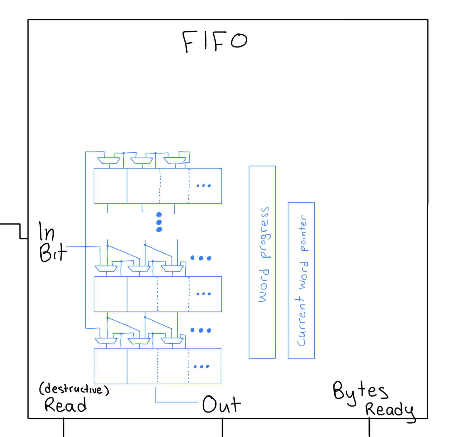
FIFO
I designed the FIFO such that a random bit can be shifted in at the same time as reading and loading down to increase performance. A word in the FIFO can have a random bit shifted in, loaded from the word above, or loaded diagnlly from the word above while getting a random bit shifted in at the same time, or of course just retain its value.