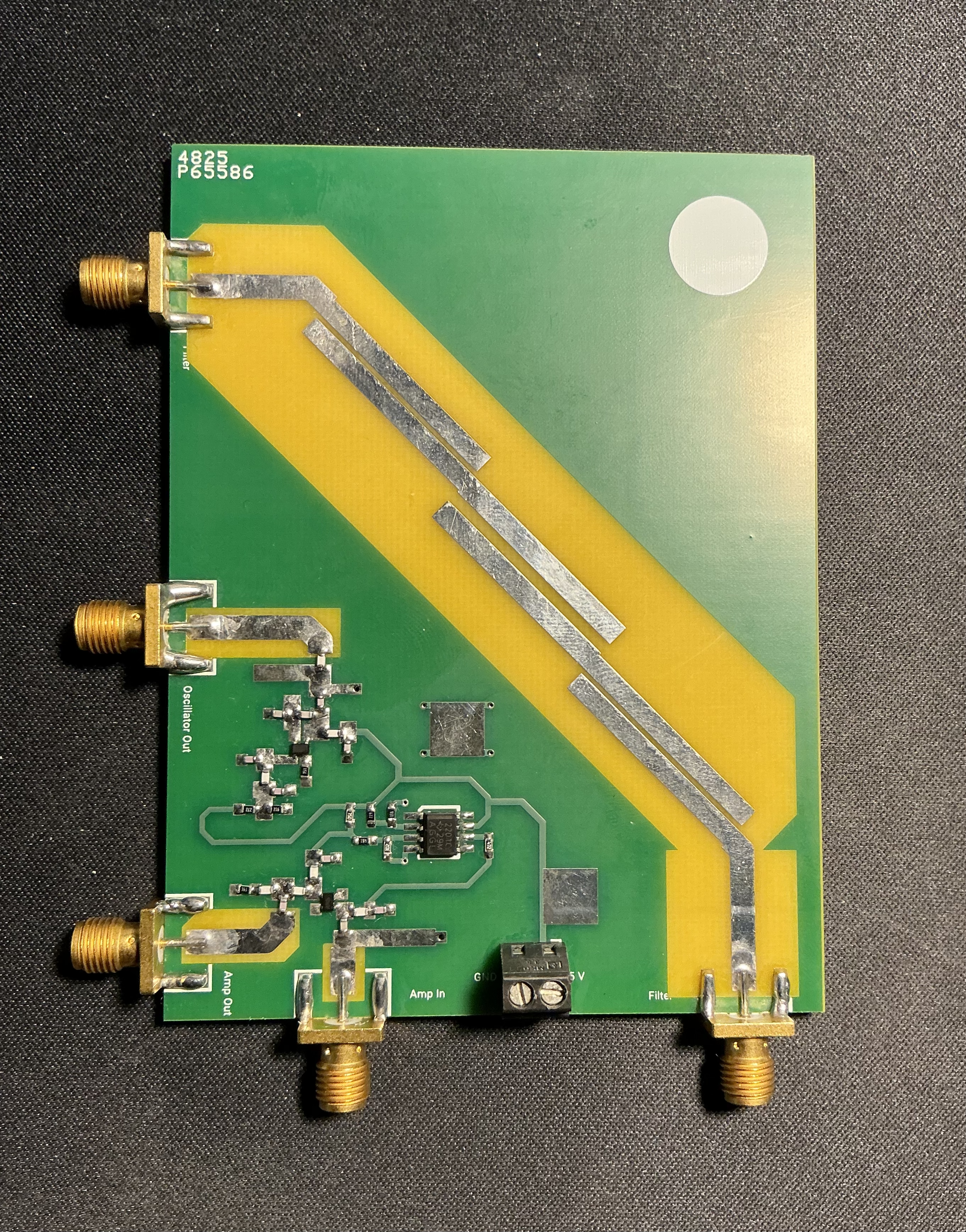
I found EE 5140 Microwave Engineering to be a great opportunity for learning analog design at the microwave and RF level. We were tasked with designing a max gain amplifier, a Colpitts oscillator, and a second order Butterworth bandpass filter. I choose a design frequency of 1.57542 GHz for all of these. That may sound like such a specific frequency, but this is the center frequency for the L1 band of GPS.
Colpitts Oscillator
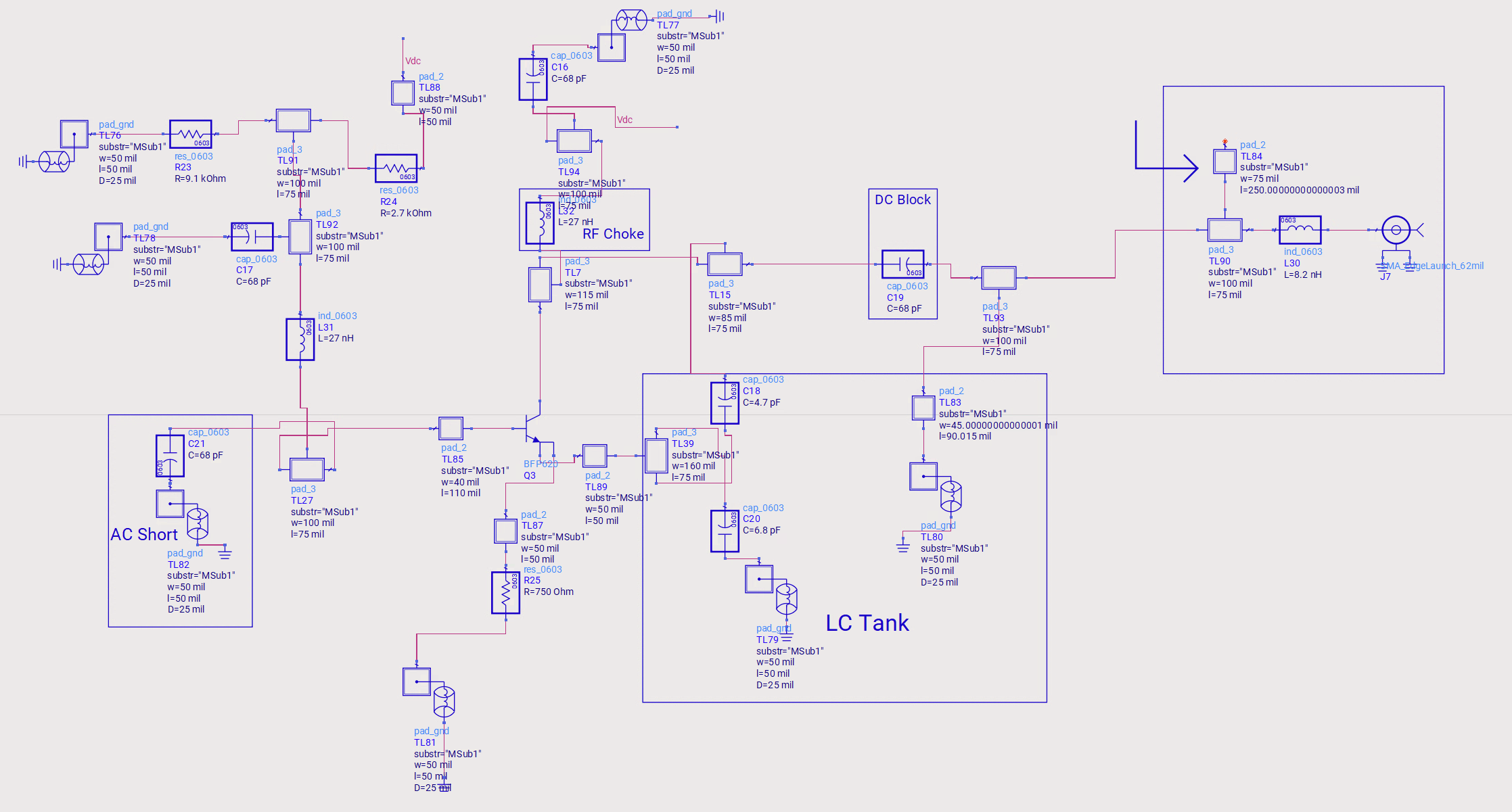
I would have to say, I was most happy with the Colpitts oscillator working as it was the most tedious in simulation land. I had even switched architectures at one point, going from common emitter to common base (which I felt was a worth while switch). This switch also allowed me to ditch having to wrap the collector to the base with a series inductor (for the LCC tank) which could have been too small an inductance for such a routing geometry to get right (the parasitic inductance of wrapping the collector to the base). The oscillator, though, in testing, was over 300 MHz off from simulation! The class is usually tasked with designing a negative resistance oscillator, but the profressor changed things up the semester I was taking it and had the people taking the 500 level version of the course design a Colpitts oscillator instead.
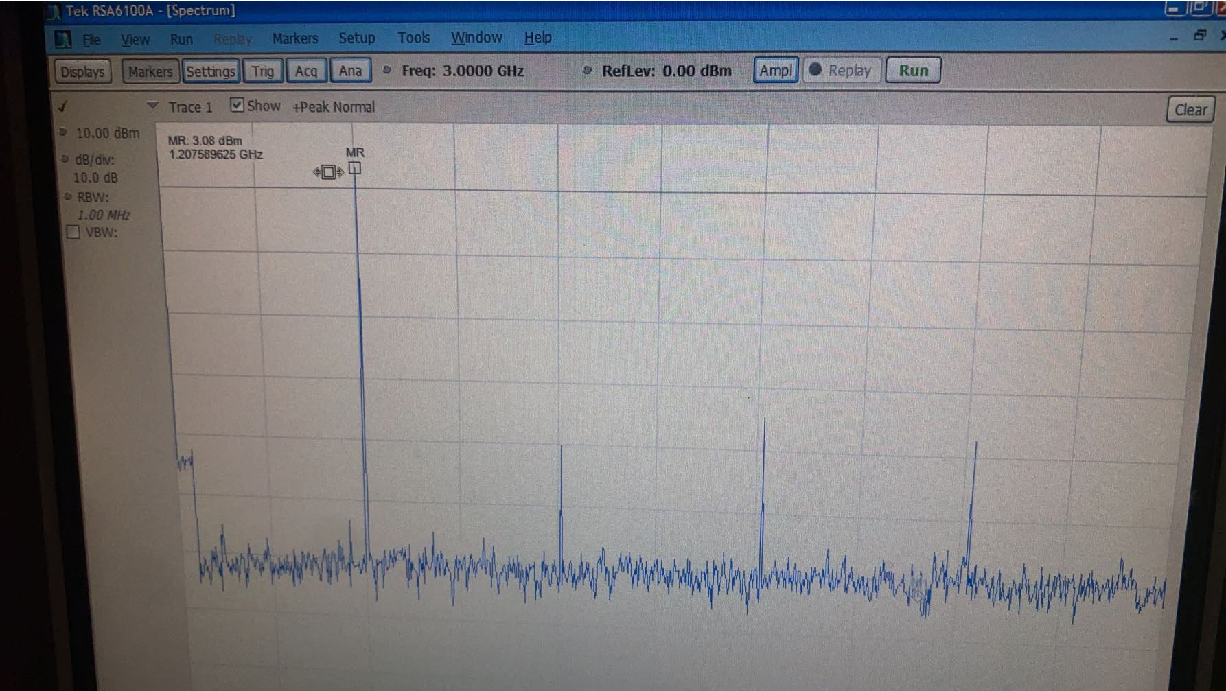
Spectral Plot of Colpitts Oscillator. 3.08 dBm @ 1.21 GHz
Max Gain Amplifier
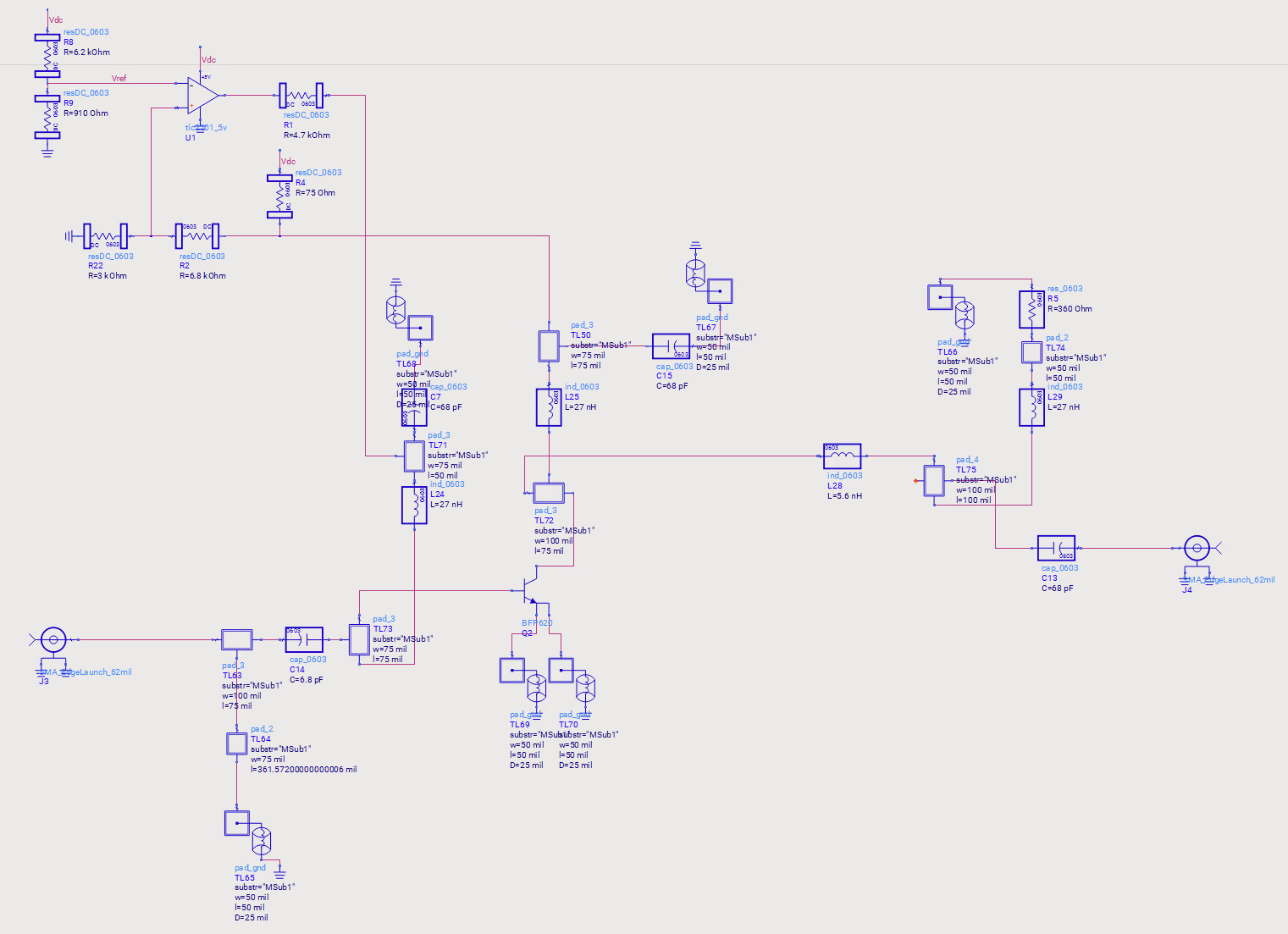
The max gain amplifier requires us to do simultaneous conjugate impedance matching. I started with L matching networks but then, at some point, swapped the shunt components with distributed components: a shunted transmission line on the source side as an inductor and an open transmission line on the load side as a capacitor. A DC bias regulator circuit was also utilized. In testing, the amplifier was at peak performance over 300 MHz off from the design frequency, operating at the same frequency as the oscillator. Them operating at the same, non planned for, frequency is great in that they are at least both compatible to be chained together with each other.
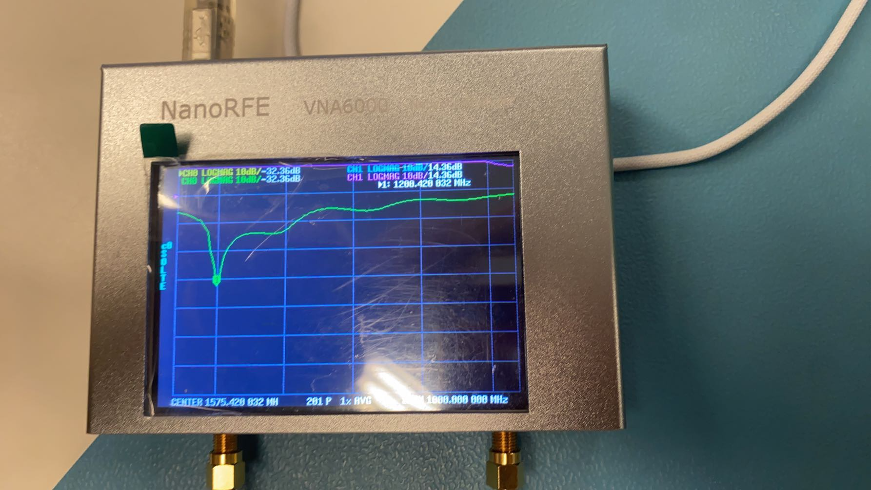
S11 (Reflection) Plot of Amplifier. 14.36 dB Gain and -32.36 dB Reflection @ 1.2 GHz
2nd Order Butterworth Band-Pass Filter
Now for the second order Butterworth bandpass filter: while the derivations for the odd and even mode characteristic impedances were, well, quite interesting; this filter was the most simple of the three to tune in simulation land and, of course, solder (which there was nothing to solder of it except the SMA connectors). The FR-4 PCB substrate was quite lossy and we incurred an insertion loss of over 4 dB. The Band-Pass center is also shifted from the desired and simulated center of 1.57542 GHz.
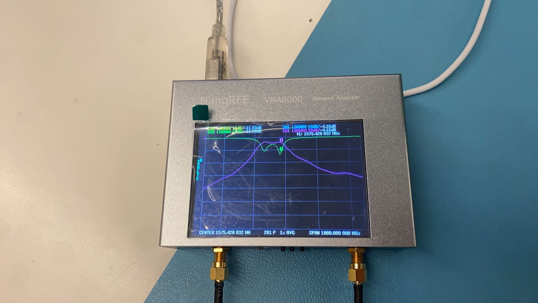
S21 and S11 Plot of Band-Pass Filter. 4 dB Insertion Loss
Here is some of the derivation of the filter (the lab assignment guided us through the steps). Of course some simulation tuning had to be done.
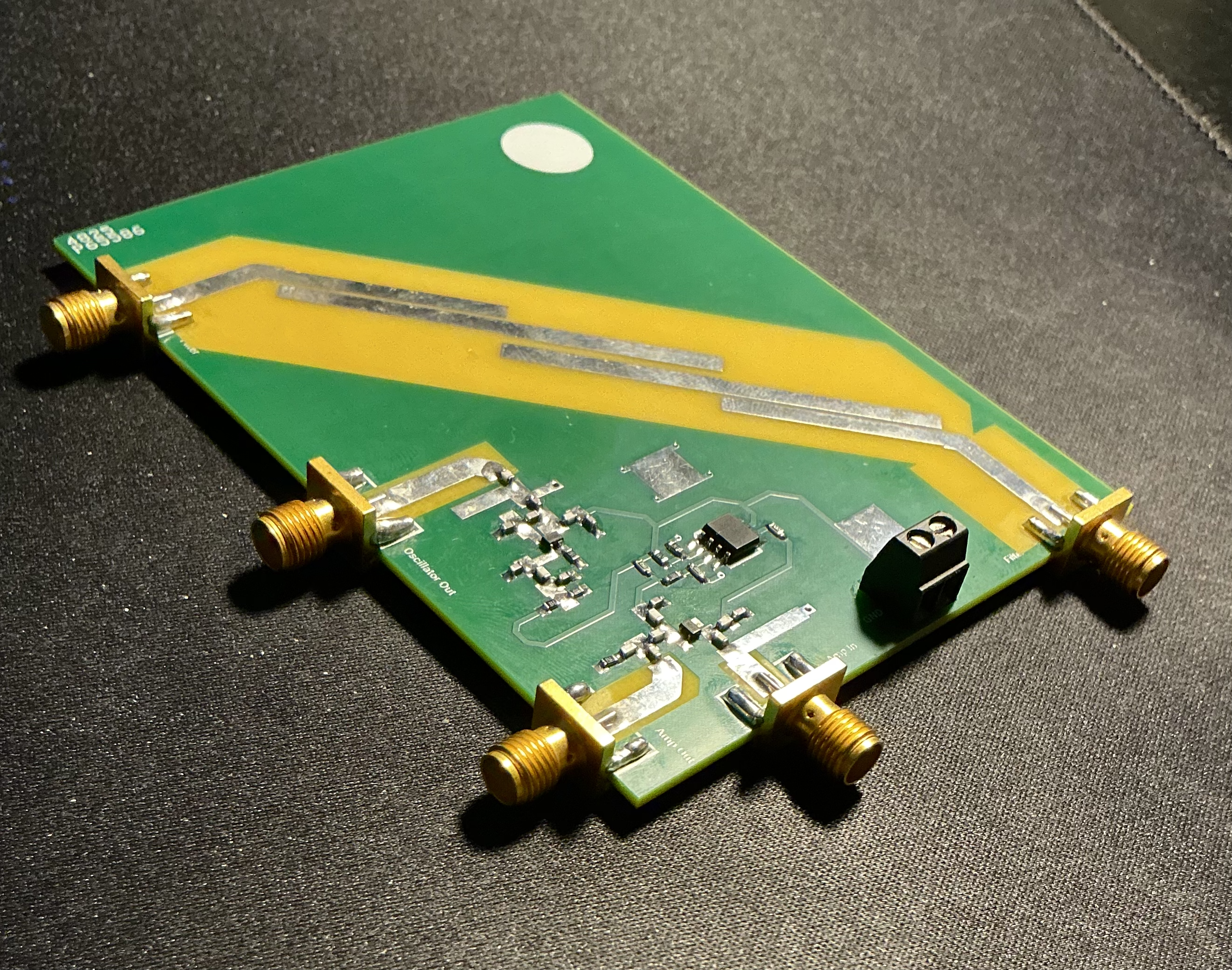
Cool Angled View